Cutting the cost of vertical MOSFETs with laser slicing
Slicing substrates with a 532 nm laser promises to trim the cost of producing GaN power MOSFETs without compromising performance
GaN vertical MOSFETs are very promising power devices for electric vehicles, having the upper hand over SiC equivalents in channel mobility, a key metric. However, commercial success is held back by the high cost of the native substrate.
To address this concern, a number of teams have been investigating technologies for recycling GaN substrates. They include a collaboration between researchers at Mirise Technologies, Nagoya University and Hamatsu, that is claiming to have produced the most comprehensive demonstration of success with this approach.
According to team spokesman Takashi Ishida from Mirise, previous reports of recycling GaN substrates have been limited to evaluating just part of the process. “It is indispensable to evaluate the device characteristics fabricated on a recycled wafer,” argues Ishida, “and our paper reported this result for the first time.”
Ishida adds that while their result is encouraging, there’s more work to do before their process can be applied on an industrial scale. As GaN substrates need to be recycled multiple times to drive down manufacturing costs, there is a need to prove that devices are not compromised when grown on substrates produced from several rounds of recycling.
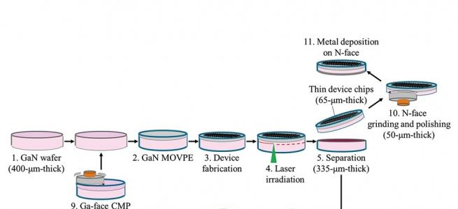
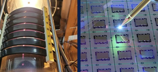
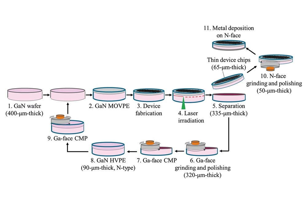
The Japanese partnership’s recycling process, outlined in the figure, involves separating the device and substrate with a 532 nm laser. This source, irradiated onto the substrate from the N-face, drives decomposition into metallic gallium and nitrogen via two-photon absorption at the focal plane.
Following separation, the N-face of the chips are ground and polished to obtain smooth surfaces, prior to metal deposition and mounting into packages.
Grounding and polishing is also applied to the Ga-face of the released substrate, prior to chemical mechanical polishing to realise flatness at the atomic level, followed by HVPE, used to deposit a layer of GaN with a thickness of around 90 μm. According to the team, after an additional chemical mechanical polishing step, the GaN substrate is as good as new.
To assess their process, the team have measured lateral MOSFETs and vertical p-n diodes fabricated from the same wafer. Both classes of device have been formed from epiwafers produced during the MOCVD of: a 4 μm-thick n-type GaN layer, doped to 1 x 1017 cm-3; followed by a 2 μm-thick p-type GaN layer, doped to 5 x 1017 cm-3.
This study began by evaluating the performance of both classes of device before and after slicing from a GaN substrate. Plots of the MOSFET drain and gate current at various gate voltages, and diode reverse currents under different values of reverse bias, showed no apparent changes due to laser slicing. This led the team to conclude that the devices are ‘virtually unaffected’ by the slicing process, which can lead to heating from the laser source and stress associated with the separation step.
Ishida and co-workers have compared these measurements with those for lateral MOSFETs and vertical p-n diodes produced using a recycled substrate. Results are very similar, with the difference in gate leakage of the lateral MOSFET attributed to a variation in the quality of the gate insulator.
According to the team, their results show that there is no critical degradation in device performance after the GaN recycling process.
Ishida says that in addition to recycling the GaN substrate, there needs to be an increase in its size to make the cost of device production more competitive. The team are interested in demonstrating their re-cycling process with larger GaN substrates
Reference
T. Ishida et al. Appl. Phys. Express 17 0265501 (2024)